The Secrets of circuit assembly-reflow soldering
- Jun 23, 2020
- 1 min read
In the last two passages we talked about solder paste layer printing and surface mount technology, now we step ahead to get some knowledge about how to fix the components at where they were placed with SMT.
Those circuit boards with placed components will have an visual checking, or with AOI checking to see if all components are correctly placed. They are being send into the oven if nothing wrong.
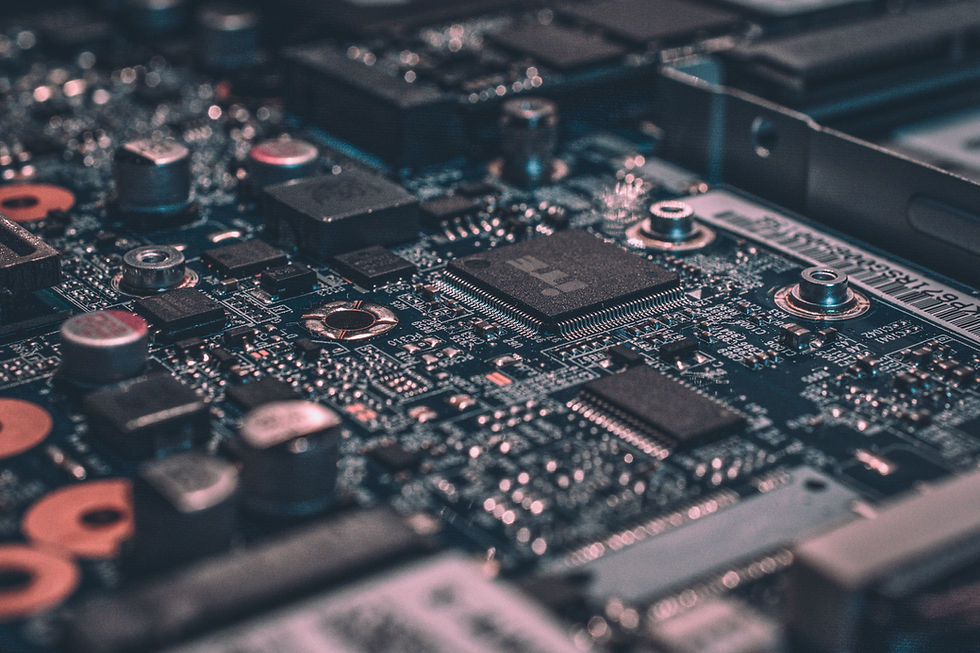
The PCB will go through a process with higher temperature which can melt the solder paste, and then reduce the temperature that the components will be fixed on the boards. The whole process will take about 8 minutes. For most of the reflow soldering oven the termperature goes up by blowing hot wind, with a number of termperature district, the highest solder paste melting district isn't that long--only tens of seconds.
So now you understand why the process is called "reflow", it means make the solder paste flowing again.

Some older people are more familier with wave soldering, it is a process designed for PCBs with DIP design, now most of the boards do not have these design, especially for IoT, automotive and advanced products, all PCBs are designed with SMT technology only.


Comments